A colour microprint containing one or more holograms
Technology title
Holographic optical element and method of forming thereof
Technology overview
Conventional optical security devices provide authentication by manipulating a specific property of light to produce a distinctive optical signature. For instance, microscopic colour prints modulate the amplitude, whereas holograms typically modulate the phase of light. However, their relatively simple structure and behaviour is easily imitated. We designed a pixel that overlays a structural colour element onto a phase plate to control both the phase and amplitude of light, and arrayed these pixels into monolithic prints that exhibit complex behaviour. Our fabricated prints appear as colour images under white light, while projecting up to three different holograms under red, green, or blue laser illumination. These holographic colour prints are readily verified but challenging to emulate and can provide enhanced security in anti-counterfeiting applications. As the prints encode information only in the surface relief of a single polymeric material, nanoscale 3D printing of customised masters may enable their mass-manufacture by nanoimprint lithography.
This technology solves the limitation of simultaneously controlling the phase and amplitude of light in conventional optical security devices. The next generation display or optical anticounterfeiting companies are the potential purchasers of these holographic colour prints. The IP realises a physical unclonable function device with a multichannel anticounterfeiting optical element.

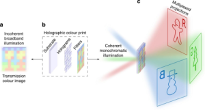
Figure 1. Structure and function of the holographic colour print, a multi-layered structure in which colour filters are stacked on top of holograms on a substrate. Under white light transmission illumination, a colour image is seen due to the arrangement of the colour filters. With laser illumination, each wavelength selects a different multiplexed holographic projection.

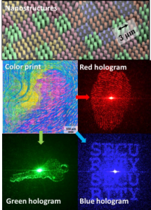
Figure 2. Color print and R, G, B holographic projections with one fabrication hologram. The optical element is formed of multilevel phase blocks with different nanopillars on the top (Scanning electron microscope image, false coloured for the corresponding wavelength). Each unit is made of one phase block with the size of 3×3 µm2 and 3×3 nanopillars atop. Under the white light illumination, one color print can be observed in the transmission mode (captured with microscope). Under laser illumination (449, 527, and 638 nm), three different holographic projections with corresponding colors can be captured on the screen.
Technology specifications
- The optical device is fabricated via two-photon polymerization lithography. The femtosecond laser is 780 nm with 90 fs pulse duration at 80 MHz repetition rate, and is focused via a 63×, NA 1.4 immersive objective. The laser power incident on the entrance aperture of the objective lens was controlled by an acousto–optic modulator.
- The material for element fabrication is a photoresist IP-Dip, while for further replication and nanoimprinting, other curable photoresists can be applied.
- The design is based on a modified Gerchberg-Saxton algorithm for far-field diffraction in transmission mode with multiple channel information encrypted.
- The area to be patterned is split into a square grid of 120×120 µm2 write fields based on the maximum undistorted field of view of the microscope objective.
- The original images for holographic projection can be colourful and grayscale, and the image for colour print is colourful.
- The number N of image with pixels N×N can be several hundreds to thousands.
- The size of each phase block representing one pixel in the image is 3×3 µm2 in the xy-plane.
- A standard glass substrate is made of fused silica, 25 mm2 with a thickness of 0.7 mm, while the optical element is possible to be fabricated on any other transparent substrate with a flat surface and an area larger than the printed size.
- Polymerised IP-Dip photoresist with a refractive index of 1.54 to 1.58 across the visible spectrum, and the block thickness determined for 2π phase modulation was 0.79 µm, 0.95 µm, and 1.17 µm at the design wavelengths of 449, 527, and 638 nm. To span the required or desired range of thicknesses and avoid unwanted shifts in filter colour at thicknesses below 0.6 µm, a thickness range of 0.6 um to 1.8 um is used.
- With a strict lower limit of 100 nm on the thickness step size, the number of phase levels used in the final prints is rounded down to 7, 9, and 11, respectively for the three wavelengths.
- For phase blocks, line scan mode is used with the hatching pitch 250 nm and slice thickness 700 nm, at femtosecond laser power of 21.0 mW for the first raster scan and 16.8 mW for the second raster scan. The laser scan speed is 8000 µm/s.
- For pillars, pulse mode is used with exposure time 0.02 – 0.04 ms, laser power 33.3 – 46.4 mW, and slice thickness 0.69 – 1.01 µm.
- The pitch of the pillar arrays is 1.0 µm. The pillar height and diameter are varied in the ranges 0.5 µm to 2.7 µm and 310 nm to 390 nm, respectively. For design wavelengths of 449, 527, and 638 nm, the pillar heights are 0.7 µm, 2.6 µm, and 1.9 µm, respectively. The pillar diameters are 380 nm, 390 nm, 390 nm, respectively.
- The slice thickness is adjusted to match the (dose-dependent) axial elongation of the point spread function of the laser spot while maintaining a vertical overlap of approximately 30% (300 nm to 430 nm depending on the size of the laser spot in the vertical direction).
- For various example embodiments, the dimensions of nanopillars: height may be in a range from 0.5 to 3.0 µm; and diameter may be in a range from 100 to 500 nm. The dimensions of nanoblocks: thickness may be in a range from 50 nm to 2000 nm; lateral size (e.g., width and length) may be in a range from 1 to 10 µm.
- To wash away the excess unexposed liquid photoresist, development should be carried out by immersion of the sample in polyethylene glycol methyl ether acetate (PGMEA) for 5 minutes and then isopropyl alcohol (IPA) for 3 minutes, followed by transfer into nonafluorobutyl methylether (NFBME) as a low surface tension solvent for the final drying step.
- For color print observation, the sample is backlit by halogen lamp illumination and measured in transmission through a 5x / 0.15 NA objective lens. The transmittance spectra are measured in a narrow cone of acceptance angles using an objective with a numerical aperture of 0.15 (a half-angle of 8.6°). The illumination numerical aperture may be limited to below 0.4 (a beam angle of up to ± 23°).
- The transmittance spectra are averaged over blocks of thicknesses 0.6, 1.0, 1.4 and 1.8 µm, and the transmittance values further are averaged over a narrow bandwidth of 4 nm centred at the wavelengths 449 nm (blue), 527 nm (green), and 638 nm (red), as well as a broadband spectral range of 450-650 nm (white).
- The overall transmission efficiency for a given channel may be the product of the area fraction occupied by the channel and the weighted average of the transmittance of the colour filters on that channel, with an upper bound of 33% for the case of equal area fractions in an RGB hologram.
- Holographic photographs can be taken at different projection distances d, with the sample placed near a white sheet of paper (d = 20 cm) and far from a white wall (d = 135 cm). The projection at d = 20 cm is much less apparent at d = 135 cm, at which the projection has expanded from 2 cm to 12.5 cm, the higher orders have faded, and the unwanted projection is now over 70 cm away from the main projection.
- The holographic projection is essentially angle-insensitive between -5° and 10° and suffers a slight decrease in brightness at -10° and 15° with little loss in quality. The projection is faintly visible at –15° and +15° and disappears as the angle is increased further. A slight asymmetry in the usable range of illumination angles might be due to a small average tilt in the pillars of 2° to 3° relative to the normal, possibly introduced during the drying step of the development process.
- The projection is bright and clear in the presence of strong background light in the room despite using only 2mW of laser power to illuminate the sample. The laser is expected to illuminate the sample at 0° normal incidence under ideal conditions for the best projection quality, while larger angles are still acceptable.
Sector
Singapore: optical anti-counterfeiting
Market opportunity
The global anti-counterfeiting market size is valued at USD 117.2 billion in 2021 and is projected to reach USD 211.3 billion by 2026, around 12.5% each year. The market is expected to witness high growth due to increasing focus of manufacturing on brand protection to reduce counterfeiting.
Developing a low-cost, easy-to-fabricate but hard-to-forge method is always pursued in the market. Gratings-based optical images/holograms are the most employed currently as they fulfill the above requirements. While these traditional optical security devices provide authentication simply by the grating effect, and their relatively simple structure and behaviour is easily imitated. Our fabricated prints can provide four channels of encrypted information, greatly enhancing security. In addition, these holographic colour prints can be mass-produced with simple nanoimprinting lithography.
Applications
The unique anti-counterfeiting properties can be employed for banknotes, credit card, passport, and secretive documents etc., also can be used for the authentication label of food, medicine, luxuries, and other products.
Customer benefits
- Multi-information: One simple device but with four channels of different information inside for authentication.
- Simple-authentication: The inspection method is remarkably simple: the image of colour print can be easily observed through the transmitted white light or under a microscope/a smartphone with transmissive illumination. The three holograms can be seen via RGB laser illumination. There is no specific requirement for high-power laser, thus laser pointer is enough. The illumination angle is not restricted.
- Mass-production: The structure is comprised of 2.5D micro-nanostructures, and the surface relief fabricated by 3D printing is readily to be used as master mold for mass-manufacture by nanoimprint lithography.
- Economic-friendly: The material for the device is based on low-refractive index materials, hence most of the transparent polymers, plastics, glasses can be employed here for low-cost fabrication. In addition, biocompatible materials like cellulose, chitosan can also be used for biomedical applications. The design can also be transferred to other refractive index materials thus the devices can be sealed to prevent damage and forging.
- Auto-algorithm: Based on the vast test, the algorithm is easy to operate by simply changing the coloor print images and projection images to any desired ones. It can efficiently provide the design in several minutes.
Technology readiness level
TRL5: Technology component and the basic technology subsystem validation in a relevant environment.
Ideal collaboration partner
The partner is expected to help the innovation step into market stably while protecting the IP rights and making sound business decisions. They can help identify new business opportunities, conduct a landscape analysis and help focus investment efforts and maximise profits. They should also help defend against emerging threats to protect IP assets and remain competitive, continually monitoring the external environment is essential.
Collaboration mode
We are happy to provide R&D collaboration, licensing, and IP acquisition as required by the potential customers.
