
Electron beam lithography with plasma-assisted filling for increased-throughput patterning with negative tone electron beam resist
Electron beam lithography with plasma-assisted filling for increased-throughput patterning with negative tone electron beam resist
Technology title
Plasma-assisted filling for electron beam lithography
Technology overview
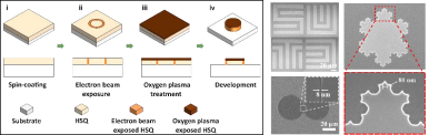
Electron-beam lithography (EBL) is a form of maskless lithography tool that is widely used in nanofabrication due to its rapid prototyping and high-resolution patterning capabilities. However, the patterning process employing EBL typically suffers from low throughput due to the patterning process of scanning across all designated pixels by a scanning-focused electron beam. This technology introduces the use of plasma treatment to increase the patterning throughput for closed polygon structures in EBL process without affecting the resolution of the patterned structures, allowing the patterning efficiency of EBL to be enhanced by 50 times and above.
This technology is potentially useful for manufacturers of beam lithography tools such as electron beam lithography (EBL) and focused ion beam lithography (FIB) to develop next generation lithography systems for high-volume fabrication equipment. In addition, this technology could also be useful in semi-conductor and nanophotonic industries for rapid prototyping of photomask and photoreticle in the fabrication process which could help improve the manufacturing cost of photomask fabrication.
Technology specifications
This technology provides a device comprising a substrate and a patterned structure formed by the method comprising:
- forming a resist layer on the substrate;
- exposing a first portion of the resist layer to a focused electron beam to form a modified first portion
- performing a plasma treatment on a surface of the resist layer, including on a surface of the second portion of the resist layer to form a modified surface portion of the second portion of the resist layer, resulting in a plasma-treated resist layer; and
- performing development of the plasma-treated resist layer to form the patterned structure on the substrate corresponding to the second portion of the resist layer.
Sector
Semiconductor
Market opportunity
The global semiconductor manufacturing equipment market was estimated at US$ 72.69 billion in 2021. It is expected to grow to US$ 122.1 billion by 2028. The market is driven by a spike in demand for consumer electronics. As per the SEMI’s World Fab Forecast issued in June 2021, 19 new high-volume fabrication facilities were built in 2021, with another 10 high-volume fabrication facilities expected to be built in 2022. Thus, the growing demand for semiconductor fabrication facilities provides lucrative opportunities for the global semiconductor manufacturing equipment market.
Applications
It can be used for a wide range of nanostructured devices including but not limited to electronic devices, opto-electronic devices, quantum structures, metamaterials, transport mechanism studies of semiconductor/superconductor interfaces, microelectromechanical systems, optical, and photonic devices.
Customer benefits
- Only need to write the boundary of the structure during electron beam writing process and still get a full polygon structure.
- Reduce the writing time of electron beam process by 50 times and still get the full structure.
- Significant improvement to the patterning efficiency.
IP status
US and Singapore Patent applications
Stage of development
TRL 3