A photonics breakthrough: Printing 3D photonic crystals that completely block light
A multi-institutional research team led by SUTD has developed a novel method that uses titanium resin to fabricate high-resolution 3D photonic crystals with a complete photonic bandgap in the visible range—a feat that has eluded scientists for decades.
Photonic crystals are materials with repeating internal structures that interact with light in unique ways. We can find natural examples in opals and the vibrant coloured shells of some insects. Even though these crystals are made of transparent materials, they exhibit a “photonic bandgap” that blocks light at certain wavelengths and directions. A special type of this effect is a “complete photonic bandgap,” which blocks light from all directions. This complete bandgap allows for precise control of light, opening up possibilities for advancements in telecommunications, sensing, and quantum technologies. As a result, scientists have been working on different methods to create these advanced photonic crystals.
While 1D and 2D photonic crystals have been used in various applications, unlocking the secret to producing 3D photonic crystals with a complete photonic bandgap in the visible range has been fraught with challenges due to the need to achieve nanoscale precise control of all three dimensions in the fabrication process.
This is all set to change. In a groundbreaking study, “Printing of 3D photonic crystals in titania with complete bandgap across the visible spectrum” published in Nature Nanotechnology, researchers across institutions in Singapore and China have achieved an unprecedented feat. Led by Professor Joel Yang from the Singapore University of Technology and Design (SUTD), the team has developed a revolutionary method to print 3D photonic crystals using a customised titanium resin.
Unlike in previous attempts, this new method has resulted in crystals that are of high resolution, possess a high refractive index, and feature a complete bandgap across the range of visible light. The innovation holds immense potential for transforming industries.
“For decades, researchers have been trying to produce photonic crystals that completely block light in the visible range. These crystals will have potential use in the elaborate 3D control of light flow, the behaviour of single-photon emitters, and quantum information processing,” explained Dr Zhang Wang, SUTD research fellow and first author of the paper.
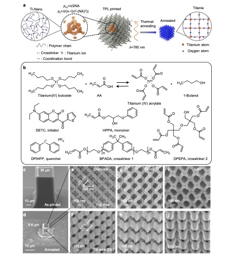
The SUTD team fabricated their 3D photonic crystal by drawing upon multiple disciplines like material science, optics, and fabrication techniques. To print the crystals, the team turned to two-photon polymerisation lithography (TPL), a technique used in additive manufacturing. Commercially available resins used in TPL printing are made of organic materials that have a low refractive index. This meant that it would be impossible for any printed structure to block the complete spectrum of visible light.
Titanium dioxide, on the other hand, is an inorganic material with a very high refractive index. In fact, titanium dioxide, also known as titania, is already being exploited in other fields for its optical properties. “It is used for its whitening properties due to light scattering from titania particles, and is found in common consumer items such as toothpaste and sunscreen and in self-cleaning surfaces,” said Prof Yang.
The team first developed a custom-made titanium resin, then printed photonic crystals using standard TPL before heating them in air to remove organic components from the crystals. The heating process also oxidised the titanium ions within the crystals, turning the ions into titanium dioxide, i.e. titania.
“The structure of the crystals shrinks by approximately six times during the heating process, and its pitch can become as small as 180 nm after shrinkage,” said Dr Zhang. The pitch refers to the distance between different layers within the printed crystal; the smaller the pitch, the more enhanced the resolution.
After successfully fabricating the photonic crystals to a very high resolution, the team observed a complete photonic bandgap across the visible range in these 3D structures. This opens up many possibilities: such structures can be used for applications like colour generation and wave guides. In addition, the customisability inherent to TPL means that the printed crystals can be modified for specific purposes, such as by introducing intentional defects within the structures.
The research team envisions broader applications beyond the creation of 3D photonic crystals. The successful development of this 3D printing technique, utilising titanium resin to achieve a complete photonic bandgap in the visible spectrum, represents a significant breakthrough in the field of photonics.
According to Dr Zhang, the process holds promise as a versatile platform for fabricating diverse materials—including glass, ceramics, and metals—at the nanoscale. This versatility is expected to create new avenues of exploration as researchers experiment with different materials and nanostructure configurations.
“This collaborative study pushed the boundaries of material science and nanofabrication process design and technologies,” added Prof Yang. “It also reflects SUTD’s mission to draw on multiple disciplines to make a positive impact on society.”
Acknowledgements:
J.K.W.Y. acknowledges National Research Foundation (NRF) Singapore (NRF-CRP20-2017-0004 and NRF-NRF106-2020-0005). S.T.H. acknowledges the funding support from MTC-Programmatic (Grant No.: M21J9b0085) administered by A*STAR. H.L.L. acknowledges the A*STAR Career Development Fund (222D800032). The authors acknowledge the support from Texas A&M University, Prof Edwin L. Thomas for discussion of this work.
Reference:
Printing of 3D photonic crystals in titania with complete bandgap across the visible spectrum, Nature Nanotechnology (DOI: 10.1038/s41565-024-01780-5)

Figure 1. (a) Schematic of the fabrication process. (b) Scanning electron microscope (SEM) image of an as-printed diamond PhC. (c) Tile view SEM image of the annealed diamond PhC. (d-i) High-magnification SEM images of the top and tilt view of the annealed diamond (d-e), gyroid (f-g) and I-WP (h,i) PhCs, respectively.
