Advancing photonics materials with cellular automation
Materials Design, Photonics, and Data Storage
SUTD – Yunzheng Wang, Jing Ning, Li Lu and Robert E. Simpson
NUS – Michel Bosman

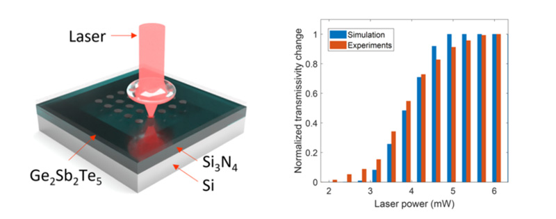
(Left) Schematic diagram of the Ge2Sb2Te5 programmable optical stack. (Right) Simulated and measured normalised transmissivity change at 300 ns laser pulses width different laser powers.
Researchers from the Singapore University of Technology and Design (SUTD) have designed a novel computational model that accurately predicts the properties of photonics materials, paving the way for next-generation photonics devices. Their findings, published in npj Computational Materials, could lead to futuristic holographic displays, enhanced LiDAR sensors for reliable self-driving cars and better machine learning capabilities via all-optical neural networks.
Pioneered in the 1960s, photonics refers to the ability to harness, generate, detect and transmit fundamental light particles called photons and light waves. Since then, photonics has revolutionised fields like telecommunications, with fibre optic cables enabling the high-speed, high-bandwidth transfer of data even across great distances.
Typically, photonics materials have fixed properties and cannot be tuned. However, phase change materials, which were originally developed for optical data storage purposes, can be programmed to have different optical properties, for example reflecting or absorbing.
For new photonics applications, more than two optical states are needed. However, achieving such conditions can be easier said than done. “Optimising the programming conditions to create different phases is challenging, time-consuming and tedious,” said study leader Associate Professor Robert Simpson from SUTD’s Engineering Product Development pillar.
Before the onset of COVID-19, Assoc Prof Simpson shared that his team had been leveraging experimental techniques to design and develop photonics computational materials (PCM) with two or more optical states. Taking inspiration from the late mathematician John Conway, who devised ‘The Game of Life’ in the 1970s, the team sought to explore instead how cellular automation could help design PCMs with multiple optical phases.
“Cellular automation is a way to model interacting cells,” explained Assoc Prof Simpson. “When thousands of cells interact, the collective behaviour of a simple system becomes complex and interesting patterns emerge.”
Accordingly, Assoc Prof Simpson and his colleagues used cellular automation to simulate the crystallisation of the PCM Ge2Sb2Te5 under certain conditions. “We showed that the model accurately predicts the laser pulses required to partially switch PCMs and produce a wide range of optical states,” he added. To the team’s surprise, they found that Ge2Sb2Te5 exhibited growth-dominated crystallisation instead of being governed by nucleation, and this effect is important because the optical response of photonics devices can be tuned to multiple optical levels via crystal growth.
As the first model of its kind to simulate multi-level phase change switching, the research team has made its code open source to encourage other researchers to develop and optimise other programmable photonics materials.
“Moving forward, we are also developing new PCMs that are transparent in the visible spectrum, instead of those that are non-transparent, such as Ge2Sb2Te5,” concluded Assoc Prof Simpson. “Transparency is key in enabling futuristic applications like holographic displays.”
Acknowledgments:
This research was supported by the NSLM project (A18A7b0058). Support from A*STAR’s microscopy facility is kindly acknowledged. Ms Ning is grateful for her Singapore Ministry of Education (MoE) PhD scholarship. We are thankful for the compute time granted by the National Supercomputing Centre (NSCC) Singapore. The work was carried out under the auspices of the SUTD-MIT International Design Center (IDC).
Reference:
A scheme for simulating multi-level phase change photonics materials. npj Comput Mater 7, 183 (2021). (DOI: 10.1038/s41524-021-00655-w)
