LEGO stacking of 2D materials brings us a step closer to ultracompact memory and spintronic tech
SUTD - Ricky L. K. Ang, Yee Sin Ang
Hengyang Normal University, China - Liemao Cao and Xiaohui Deng
Hunam Normal University, China - Guanghui Zhou
Nanjing University, China - Shi-Jun Liang
Le Quy Don Technical University, Vietnam - Chuong V. Nguyen
SUTD scientists designed a novel functional 2D hybrid material for ultracompact memory and spintronic device applications.
The continuous miniaturisation of electronic devices has led to the innovations of more powerful, compact devices. These electronic devices, such as smart phones and laptops, are the key enablers of many ground-breaking technologies including artificial intelligence, social networks, tele-medicine and 5G networks. They have transformed the 21st century into a smarter and more interconnected world more than ever before.
The shrinking of electronics into the nanometer regime – a scale of length where a single nanometer is roughly ten thousand times thinner than a strand of human hair– also brings tremendous technological challenges.
Silicon, a key building block of modern electronics, starts to behave in an erratic manner due to the onset of bizarre quantum mechanical effect that dominates the nanoscopic world. Silicon nanoelectronics thus must be thinned down substantially, so that the quantum effect can be tamed to allow for better control over the device. The fabrication of silicon nanoelectronics, however, are technologically demanding. The electrical properties of silicon oftentimes can become severely degraded if the ‘thinning down’ process is not carried out properly.
Two-dimensional (2D) materials – an ultra-thin material family with a thickness of no more than a few atoms – provide new opportunities for continuing the never-ending quest of electronic device miniaturisation.
Due to its inherently ultra-thin body, 2D material devices have excellent controllability even at the nanometre scale. Scientists and engineers have demonstrated their potential in myriads of advanced device technologies applications, including faster, less energy-hungry, flexible, highly compact, and even brain-mimicking devices.
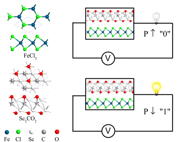
More intriguingly, different species of 2D materials can be ‘LEGO-stacked’ into a van der Waals heterostructure (vdWH) (refer to image 1). The physical properties of the constituent materials are fused together, leading to new ‘designer’ physical properties which are not easily found in natural crystals.
The vdWH approach greatly expands the functional device design flexibility of 2D materials. One particularly interesting and technologically important class of vdWH is the multiferroic variant, in which 2D materials with fundamentally different physical properties are combined.
 The crystal structures of FeCl2 and Sc2CO2 monolayers (left panel) and the schematic illustrations of how the LEGO stack of FeCl2 and Sc2CO2 can be used for digital information, ‘0’ and ‘1’, processing (right panel).
For example, a magnetic 2D material can be combined with another ferroelectric 2D material whose electrical behaviour can be tuned externally via a voltage signal. The resulting multiferroic VdWH can then offer voltage switchable magnetism – a behaviour tremendously useful for computing electronics and memory devices.
Whether multiferroic vdWH can be successfully constructed depends critically on appropriate materials selection. Although 2D-material-based multiferroic vdWH is much sought after, the extensive search of functional multiferroic vdWH has only resulted in a few prototypes with sufficiently good potentials for electronics device application.
The research team led by the Singapore University of Technology and Design (SUTD) designed a multiferroic vdWH with strong capability in memory and spin-based computing applications using state-of-art computational simulation. By stacking FeCl2 monolayer – a magnetic 2D material – and on of Sc2CO2 – a ferroelectric 2D material, the team found that the magnetism of the resulting multiferroic vdWH could be easily switched using a voltage signal.
Based on comprehensive and rigorous computational search, the most optimal stacking configurations and material combinations are obtained. These findings can provide useful design guidelines for subsequent experimental fabrication, device prototyping and advance spintronic technology.
Spintronics is an emerging device concept that operates on a radically different principle compared to traditional electronics technology. By exploiting the ‘spin’ of an electron – an intricate quantum mechanical property, spintronic devices are expected to enable ultrafast computation while consuming much less energy. Based on a nanodevice simulation, the research team demonstrated that the multiferroic vdWH designed in this work could be operated as spin polarizers – a crucial building block of spintronic technology.
“Although multiferroic systems have been widely studied using bulky materials, the 2D material counterpart studied in this work has the potential of ultimately compact multiferroic devices, which could be very useful for ultracompact memory devices. The ability to host a spin-polarised current further suggests that the system can also be a candidate material for spintronic technology,” said Dr Yee Sin Ang, an Assistant Professor at SUTD who led this study.
“The multiferroic vdWH designed in this project offers an interesting route for the development of high-performance computing electronics with minimal energy consumption, thus paving an important first step towards a more sustainable future computing electronics technology,” added Ang.
Acknowledgements:
L.C. is supported by the National Natural Science Foundation of China (Grant No. 12104136) and by the Scientific Research Fund of Hunan Provincial Education Department (Grant No. 21B0622). G.Z. acknowledges the support of National Natural Science Foundation of China (Grant No. 12174100). Y.S.A. acknowledges the support of SUTD Startup Research Grant (Project No. SRG SCI 2021 163). L.K.A. acknowledges the support of Singapore Ministry of Education Academic Research Fund (MOE AcRF) Tier 2 Grant No. 2018-T2-1-007 and A*STAR AME IRG Grant No. A2083c0057. All calculations were carried out using the computational resources provided by the National Supercomputing Centre (NSCC) Singapore.
Reference: Multiferroic van der Waals heterostructure FeCl2/Sc2CO2: Nonvolatile electrically switchable electronic and spintronic properties, Physical Review B. (DOI: 10.1103/PhysRevB.105.165302)